
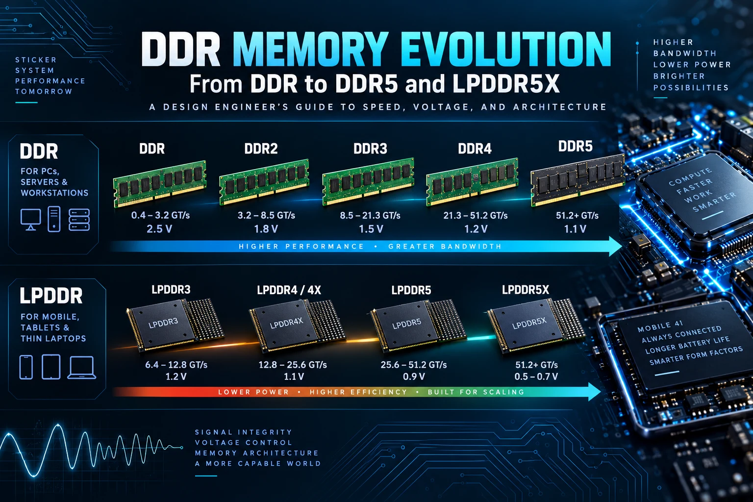
DDR memory evolution runs through five generations of standard DDR — DDR, DDR2, DDR3, DDR4 and DDR5 — plus a separate low-power line built for phones, tablets and thin laptops: LPDDR2 through LPDDR5X. Each generation roughly doubles the data rate of the one before it while lowering operating voltage and adding features that keep the memory bus stable at higher speeds. Standard DDR chases raw data rate for PCs, workstations and servers. LPDDR is a different design built around a power budget first and speed second. Picking the right standard for a new board comes down to four things: how much power the device can spend, how much board space is available, how much bandwidth the workload needs, and how much validation time the schedule allows.
What Is DDR Memory and How Does It Work?
DDR stands for Double Data Rate. It is a type of synchronous DRAM built to move data on both the rising and falling edge of the clock signal instead of just one. Older SDRAM sent one word of data per clock cycle. DDR sends two, so a chip clocked at 100 MHz reaches a data rate of 200 MT/s (million transfers per second) without raising the clock frequency at all.
That single change is the foundation every later generation builds on. DDR2, DDR3, DDR4 and DDR5 do not reinvent the double-edge trick; they widen the prefetch buffer, add more banks, lower the operating voltage, and clean up signal handling so the same trick keeps working as clock speeds climb. The prefetch buffer is worth a mention on its own: it is the number of data bits the memory chip lines up internally for each memory access. DDR uses a 2n prefetch, DDR2 moved to 4n, and DDR3 through DDR5 use 8n. A wider prefetch means the chip can serve a fast external data rate from a slower, easier-to-manage internal array, which is part of why each generation can double its predecessor’s data rate without doubling its internal clock.
DDR Memory Evolution: Generation by Generation
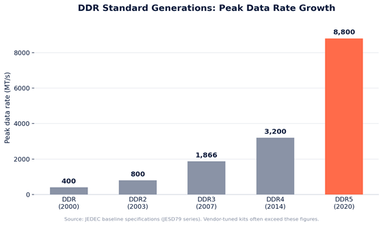
Five generations of standard DDR have shipped since 2000, each one aimed at desktops, laptops, workstations and servers.
DDR (2000)
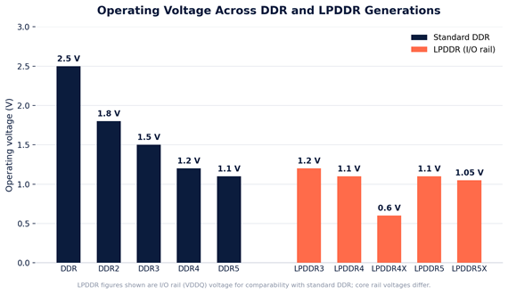
The first generation proved the double-data-rate concept at the memory level. It ran at 2.5 V and reached data rates from 200 to 400 MT/s.
DDR2 (2003)
DDR2 dropped operating voltage to 1.8 V and moved to a 4n prefetch buffer, which let it reach higher speeds without pushing the internal array as hard. Common speed grades were DDR2-400, DDR2-533, DDR2-667 and DDR2-800.
DDR3 (2007)
Running at 1.5 V, or 1.35 V for low-voltage variants, DDR3 pushed data rates from 1066 MT/s up to 1866 MT/s and became the standard across desktop PCs, laptops and servers for close to a decade. Its 8n prefetch buffer set the pattern later generations would keep.
DDR4 (2014)
DDR4 cut operating voltage again, to 1.2 V, and shipped in speed grades from DDR4-2133 up to DDR4-3200 in JEDEC’s baseline specification, with vendors pushing well past that on tuned kits. DDR4 also introduced bank groups, which split the memory array into sections that can be accessed independently and reduce the wait between back-to-back operations on the same bank.
DDR5 (2020)
DDR5 runs at 1.1 V and moved voltage regulation onto the memory module itself through an on-board Power Management IC, rather than leaving it to the motherboard. JEDEC’s baseline specification starts DDR5 at 3200 MT/s and defines speed grades up to 8800 MT/s — roughly double DDR4’s top rate — with module capacity up to four times higher. DDR5 also splits each module into two independent 32-bit sub-channels instead of one 64-bit channel, doubling the bank groups available and giving the memory controller more parallel work to schedule. On-die error correction is standard on DDR5, where it was optional or absent on earlier generations.
What Is LPDDR and Why Mobile Devices Need a Different Standard
Standard DDR is built for systems with a power supply and a fan. Phones, tablets, wearables and thin laptops have neither. LPDDR (Low Power DDR) is a separate JEDEC standard, developed alongside mainline DDR but tuned around a power budget rather than a data-rate target. It runs at a lower operating voltage, adds deep power-down and self-refresh states the standard DDR spec does not define, and is packaged directly on top of the processor package (package-on-package, or PoP) rather than sitting in a socket or slot. That packaging choice shortens the trace length between the memory and the processor, which helps both power and signal quality, but it also means the memory is fixed at manufacturing time. There is no upgrade path the way there is with a DIMM slot on a desktop board.
LPDDR Generations Explained
The LPDDR line runs from LPDDR1 through LPDDR2, LPDDR3, LPDDR4, LPDDR4X, LPDDR5 and LPDDR5X, with LPDDR6 published by JEDEC in 2025.
LPDDR3
Used across early smartphones and ultrabooks, LPDDR3 balanced performance against power draw at a point when phone processors were only just starting to need real memory bandwidth.
LPDDR4 and LPDDR4X
LPDDR4 doubled LPDDR3’s data rate to 3200 MT/s and moved to a 16-bank architecture. LPDDR4X kept the same speed grades but split the I/O voltage rail from the core voltage rail, cutting the I/O voltage to around 0.6 V and lowering power draw further. This pairing became the default for mid-range and flagship smartphones, tablets and light laptops for several years.
LPDDR5
LPDDR5 raised the data rate ceiling to 6400 MT/s, doubled bank count again to sixteen banks organised as eight bank groups, added a separate WCK clock line for cleaner signal timing at high speed, and introduced Adaptive Refresh Management, which adjusts how often the memory refreshes itself based on real-time temperature instead of a fixed schedule.
LPDDR5X
Published as an extension to the LPDDR5 spec, LPDDR5X pushes the data rate ceiling to 8533 MT/s on the same core voltage as LPDDR5, largely through better signal equalisation on the transmit and receive paths rather than a change in the base architecture. LPDDR5X also raised the maximum die capacity, which matters for on-device AI workloads that keep large models resident in memory. It is now the majority standard shipping in current flagship phones and AI-capable edge devices.
DDR vs LPDDR: The Architectural Differences That Matter for Design
LPDDR is not a slower cousin of DDR running on a lower voltage. It is a separate architecture aimed at a different constraint.
| Factor | Standard DDR | LPDDR |
| Power | Single voltage rail; no deep power-down states in the base spec | Split voltage rails (core + I/O); deep power-down and self-refresh states built in |
| Packaging | Removable DIMM / SO-DIMM | Soldered, usually package-on-package on the SoC |
| Bus / channels | 64-bit bus (two 32-bit sub-channels from DDR5) | Narrower channels (often 16-bit) run in parallel |
| Upgrade path | Replaceable after the board ships | Fixed at manufacturing time |
| Reliability feature | On-die ECC (standard on DDR5) | Adaptive Refresh Management (from LPDDR5) |
Why So Many Generations? The Engineering Challenges Behind Each Jump
Each generation exists because the previous one hit a wall that could not be pushed past by tuning the same architecture harder. Doubling the data rate does not just mean a faster clock — it means the signal has less time to settle, less margin for noise, and less room for error before a 1 gets read as a 0. Board and silicon teams working at these speeds run into the same set of problems on every jump:
- Clock timing and jitter — at gigahertz-class data rates, even a few picoseconds of clock jitter can push a signal outside its valid sampling window. Timing budgets that were generous at DDR3 speeds get tight fast by DDR5.
- Signal degradation and crosstalk — trace length, via count and layer stack-up all start to matter in ways they did not at lower speeds. A layout that worked fine for DDR3 will often fail signal integrity checks outright at DDR5 or LPDDR5X speeds without a redesign of the routing and stack-up.
- Power delivery — DDR5 moving voltage regulation onto the module, and LPDDR splitting its voltage rails, are both direct answers to power delivery getting harder to manage from a distance as speeds climb. A regulator sitting far from the memory chip on a motherboard cannot respond fast enough to keep up with modern switching transients.
- Memory training and initialisation — every boot, the memory controller and the DRAM run a sequence to line up timing, calibrate impedance and set read/write levels before any real data moves. This training sequence has grown more complex with each generation and is a common source of intermittent bring-up failures that only show up under specific voltage or temperature conditions.
- Data integrity — on-die ECC on DDR5, link ECC on LPDDR5, and tighter error-management schemes across both lines exist because higher density and higher speed both raise the raw bit error rate. Correcting more errors on-chip means fewer failures reach the system level.
Choosing the Right Memory Standard for Your Design
For teams picking a memory standard for a new product, the decision usually comes down to four factors, in this order:
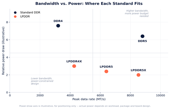
- Power budget — if the device runs on a battery and needs to sit idle for hours or days, LPDDR is close to a default choice. Its self-refresh and power-down states are not present in standard DDR at all.
- Board space and packaging — LPDDR’s package-on-package mounting saves board area and shortens routing, which matters on small form-factor products. DDR’s socketed or soldered DIMM form factor needs more board area but keeps memory replaceable and upgradeable, which matters for servers and workstations expected to be reconfigured over their service life.
- Bandwidth versus cost — at the top end, DDR5 and LPDDR5X sit close together on peak data rate, so bandwidth alone rarely settles the choice. Cost per gigabyte, available die capacities from your chosen vendor, and second-source availability usually matter more once bandwidth needs are met.
- Validation risk and schedule — a design carrying its first high-speed memory interface should budget real time for signal integrity simulation and lab validation, not treat it as a formality. Teams that have shipped DDR4 designs before still see new timing and power delivery problems moving to DDR5 or LPDDR5X, because the margins are tighter at every step.
A rough rule of thumb: standard DDR for anything with a power supply, a fan, and a socket where the memory might need to change over the product’s life; LPDDR for anything battery-powered, thermally constrained, or built around a fixed bill of materials where the memory is soldered once and never touched again. Products that sit in between — small industrial computers, some automotive modules, certain networking appliances — are where the choice gets harder and usually comes down to the SoC vendor’s supported memory interface rather than an open choice between the two.
Common Integration and Validation Challenges We See
Working on DDR and LPDDR interfaces across board bring-up and pre-silicon verification, a few failure patterns come up often enough to be worth naming directly, rather than leaving them as a generic warning.
Memory training that passes in the lab but fails in the field
Training sequences are usually run and checked at room temperature on the bench. A design with tight timing margin can pass every bring-up test and still fail intermittently once units ship into hotter or colder environments, because the margin that looked fine at 25°C was never checked at the temperature extremes the product will actually see.
Routing that looks clean but fails an eye diagram
Length-matching and impedance control can look correct in the layout tool and still fail signal integrity validation once measured with an oscilloscope, usually because of a via transition, a reference plane split, or a connector the simulation model did not capture accurately.
Power sequencing mistakes on DDR5’s on-module regulation
Moving voltage regulation onto the DIMM changes the power-up sequence the host board has to follow. Boards designed with DDR4 sequencing assumptions carried over sometimes bring DDR5 modules up in the wrong order, which can cause boot failures that look like a bad memory chip when the real fault is upstream in the power sequencing.
Treating LPDDR as a smaller DDR part in early architecture decisions
LPDDR’s narrower, parallel channel structure needs pin planning specific to the chosen SoC’s memory controller from the start of the layout. Teams that treat it as a drop-in low-power DIMM substitute often find the pin count and channel count do not match what they assumed at the schematic stage, which forces a rework late in the design.
None of these are unusual or hard to catch — they are standard items on a memory interface checklist. They show up when a schedule compresses the signal integrity and bring-up validation phases, not when the underlying engineering is unfamiliar.
Frequently Asked Questions
Is DDR5 backward compatible with DDR4?
No. DDR5 uses a different pin layout, a different voltage, and on-module voltage regulation that DDR4 boards and controllers do not support. A DDR5 module will not fit in a DDR4 slot, and a memory controller built for one generation cannot address the other.
Can I use LPDDR5X in a design that also needs a standard DIMM slot?
Not directly. LPDDR is soldered to the board and does not come in a DIMM package, so a design needing a removable, upgradeable memory slot has to use standard DDR. Some SoCs support both interfaces on separate pins, which lets a board offer soldered LPDDR for a base configuration alongside a DDR DIMM slot for expansion — but that is a platform decision made early, not a late substitution.
Why does DDR5 need a PMIC on the module instead of on the motherboard?
At DDR5’s speed grades, a voltage regulator sitting on the motherboard is too far from the memory chip to respond fast enough to fast switching current changes. Moving the regulator onto the module itself shortens that distance and keeps the voltage stable during the current transients that come with faster switching.
What's the real difference between LPDDR5 and LPDDR5X?
LPDDR5X is an extension of the LPDDR5 specification, not a separate architecture. It raises the peak data rate from 6400 MT/s to 8533 MT/s mainly through better signal equalisation on the transmit and receive paths, while keeping the same core voltage and most of the underlying design. Adaptive Refresh Management, introduced with LPDDR5, carries over and applies to both.
Does a higher DDR generation always mean better performance for my product?
Not automatically. A newer generation raises peak bandwidth, but a design only benefits if the processor, memory controller and workload can actually use that bandwidth. Moving to DDR5 or LPDDR5X without a workload that needs the extra bandwidth mainly adds validation time and part cost without a matching gain in real performance.
How much lead time should I plan for a first DDR5 or LPDDR5X memory interface design?
Plan for meaningfully more signal integrity simulation and lab bring-up time than a DDR4 or LPDDR4X design of similar complexity, particularly if your team has not carried a design through one of these interfaces before. The extra time usually goes into stack-up planning, pre-layout simulation, and post-layout eye diagram validation rather than the schematic itself.
Final Thoughts
DDR memory evolution is really the story of the same double-data-rate trick being pushed further with each generation — lower voltage, wider internal buffers, and better signal handling, generation after generation. Standard DDR and LPDDR solve different problems: one chases raw bandwidth for systems with a power budget to spare, the other protects battery life first and treats bandwidth as the second priority. Picking between them, and getting the board design right once you have picked, is where most of the real engineering work sits.
If you are choosing a memory standard for a new board, or validating signal integrity on a DDR5 or LPDDR5X interface for the first time, our VLSI design and embedded systems teams work on exactly this kind of bring-up and pre-silicon verification for clients across the semiconductor and product engineering space.
