
FPGA design and FPGA verification are two separate engineering disciplines that share a codebase and almost nothing else. The difference between FPGA design and FPGA verification comes down to intent: design describes what the logic should do in RTL and constraints, while verification proves independently that the logic actually does it before anyone loads a bitstream onto silicon. Confuse the two and you get a project where the person who wrote a bug is also the person asked to catch it, which is roughly as reliable as marking your own exam.
On small hobby projects one engineer wears both hats and it works fine. On a product that ships, a switch line card, a medical imaging front end, an automotive sensor fusion board, that overlap becomes the reason a bug survives all the way to a field return. A missed corner case in a design review is cheap. The same bug found in a customer’s rack, after the board is populated with a ₹40,000 FPGA and shipped to another city, is not.
This piece separates the two roles cleanly: what each one produces, the tools each uses, the skills each demands, the hardware validation methods that take over where simulation stops, and where the handoff between them tends to break. If you are hiring, budgeting or scoping an FPGA programme, knowing which discipline you are actually short of changes what you spend and who you look for.
What is the difference between FPGA design and FPGA verification?
FPGA design is the act of creating the hardware description: writing RTL in Verilog, SystemVerilog or VHDL, defining timing constraints, and running synthesis and place-and-route so the logic fits and meets timing. FPGA verification is the independent act of proving that RTL matches its specification, using testbenches, assertions, stimulus and coverage metrics, usually before any hardware exists.
Design produces the thing; verification produces the evidence it works.
The cleanest way to hold the two apart is by their deliverable. A designer’s output is a bitstream that a device can load and run. A verification engineer’s output is a report: what was tested, what passed, what coverage was hit, and what risk remains. One builds. The other decides whether what was built is trustworthy enough to release. That split is the practical difference between FPGA design and FPGA verification, and it drives everything from tooling to who you hire.
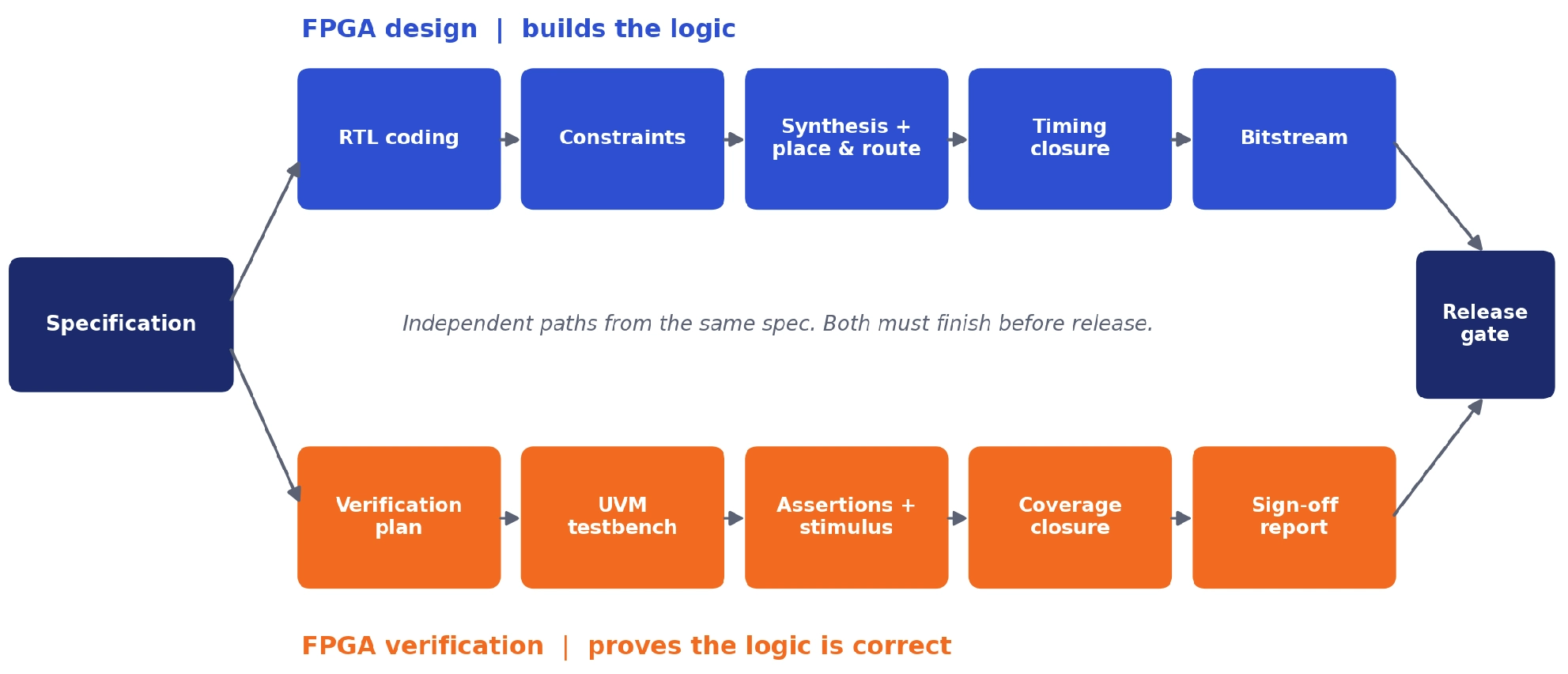
Design and verification start from the same specification and run as independent paths. Release needs both a bitstream and a sign-off report.
Quick facts
Design output: RTL, constraints, synthesised netlist, bitstream |
Verification output: testbench, coverage report, sign-off metrics |
Design languages: Verilog, VHDL, SystemVerilog |
Verification languages: SystemVerilog/UVM, plus Python and C |
The design discipline
FPGA design starts from a specification and ends with configured hardware. A designer reads the requirement, partitions it into modules, writes register-transfer-level code that describes registers, combinational logic and state machines, then drives that code through the vendor toolchain. On a Xilinx or AMD part that toolchain is Vivado; on an Intel/Altera part it is Quartus Prime. Synthesis turns RTL into gates, place-and-route maps those gates onto the device’s lookup tables, flip-flops and DSP slices, and the timing engine reports whether every path closes within the clock period.
Much of a designer’s real skill sits in the constraints, not the RTL. A clock declared at 200 MHz that the tool cannot route, a false path left unconstrained, an unregistered cross-clock-domain signal, these are design problems that show up as timing failures or metastability, not as a functional bug in simulation. A designer who understands the fabric plans with it: pipelining a wide multiplier, inferring a block RAM instead of distributed logic, budgeting fan-out so a high-priority net does not blow the timing.
Design is also where architecture lives. Choosing a 128-bit AXI datapath over a 64-bit one, deciding whether a FIFO sits in block RAM or UltraRAM, splitting a design across multiple clock islands, all of that is design intent that verification later has to test against. Get the architecture wrong and no amount of testbench effort will save you; the constraint has to be right in the RTL first. The formal semantics of these languages are set by standards such as IEEE 1800 for SystemVerilog, which both disciplines rely on to agree on what the code actually means.
The verification discipline
FPGA verification exists because a design that compiles and meets timing can still do the wrong thing. Verification builds an independent model of what correct behaviour looks like and then tests the design against it. The dominant methodology is UVM, the Universal Verification Methodology, a SystemVerilog class library that structures a testbench into drivers, monitors, scoreboards and sequences so that stimulus generation and result checking are reusable and constrained-random rather than hand-written vectors.
A verification engineer thinks in terms the designer often does not: what happens at the boundary, when a FIFO is exactly full, when two requests arrive on the same cycle, when reset asserts mid-transaction. They write assertions, often in SystemVerilog Assertions, that flag a protocol violation the instant it occurs rather than three thousand cycles later when the symptom appears. And they measure. Functional coverage answers a question the designer cannot answer honestly about their own code: have we actually exercised every state, every corner, every legal combination the spec allows?
The same discipline shows up wherever a protocol has to be proven correct rather than merely present, which is why teams treat something like USB protocol verification as its own workstream rather than a checkbox at the end of design. A verification engineer starts from the specification and works backward to the ways the RTL could betray it, which is a different mental habit from building the RTL in the first place.
Different tools, different failure modes
Design and verification reach out to different software, and the tools reveal what each job is really about. A designer lives inside the vendor implementation flow; a verification engineer lives inside a simulator and a coverage database. Both run simulation, but the centre of gravity differs.
Aspect | FPGA design | FPGA verification |
Main goal | Make the logic exist and meet timing | Prove the logic is correct |
Main tools | Vivado, Quartus Prime, synthesis, PnR | QuestaSim, VCS, Xcelium, coverage tools |
Languages | Verilog, VHDL, SystemVerilog | SystemVerilog/UVM, Python, C |
Main metric | Timing closure, resource utilisation | Functional and code coverage |
Deliverable | Bitstream and netlist | Verification report and sign-off |
Typical failure | Path fails timing, LUTs overflow | Corner case wrong, coverage hole |
The failure modes matter as much as the goals. A design failure is loud and early: the tool refuses to close timing, or utilisation hits 105 percent and place-and-route errors out. You cannot ship without noticing. A verification failure is quiet and late. The design builds, loads and runs the happy path in a demo, and the bug hides in a state combination nobody exercised until a customer’s traffic pattern found it.
That asymmetry is why verification usually consumes more calendar time and often more headcount than design on intricate parts. Writing a state machine takes an afternoon. Proving it handles every reset, overflow and back-to-back transaction can take weeks, and the effort scales with the number of interacting features rather than lines of code. A designer measures progress in modules completed; a verification engineer measures it in coverage points closed, and those two curves rarely move at the same pace.
FPGA validation methods: testing the design on real hardware
FPGA validation is the stage where a design stops running in a simulator and starts running on physical hardware. Verification asks whether the RTL matches its specification; validation asks whether the whole system behaves correctly at real clock speeds, with real software and real interfaces attached. Teams typically rely on four methods: prototyping and emulation, hardware–software co-verification, real-world interface and stress testing, and FPGA-in-the-loop testing.
Validation does not replace simulation. A UVM testbench still gives the best view of internal signals, and a bug costs far less to debug there. What simulation cannot give you is speed. A full SoC model in a software simulator often runs at a few hundred hertz to a few kilohertz, so booting an operating system or pushing a million Ethernet frames through it is out of reach. The same RTL mapped onto an FPGA runs thousands of times faster. That is also why ASIC and SoC teams use FPGAs as pre-silicon platforms, a use case our ASIC vs FPGA comparison covers from the product-decision side.
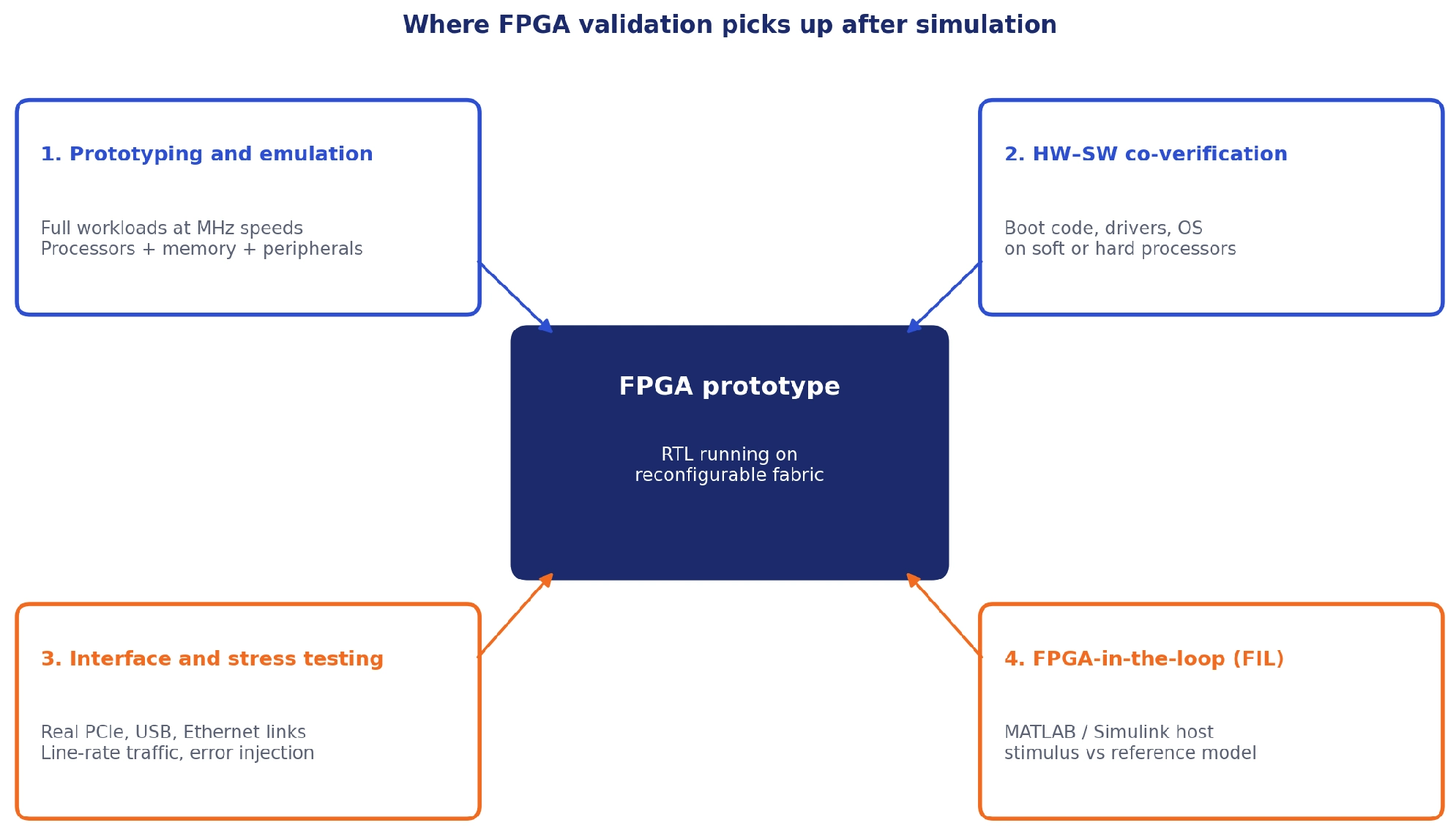
The four FPGA validation methods each connect something real to the prototype: full workloads, production software, live interfaces or an algorithm model.
1. Prototyping and emulation
An FPGA prototype maps the RTL onto reconfigurable fabric so the design runs far closer to its target speed, typically tens of megahertz for a large SoC split across one or more big FPGAs. At that rate, engineers can run full workloads instead of short directed tests. Enterprise prototyping platforms let a team check how processors, memory subsystems and peripherals behave together under sustained traffic, the kind of interaction that only shows up after millions or billions of cycles. For an ASIC programme, this work happens weeks or months before tape-out.
Dedicated emulators such as Cadence Palladium, Siemens Veloce and Synopsys ZeBu sit between simulation and FPGA prototyping: slower than a prototype, but with much better debug access. The trade-off with any FPGA prototype is visibility. Inside a simulator you can probe every signal; on an FPGA you see only what you instrumented with an on-chip logic analyser such as Vivado ILA or Quartus Signal Tap. Plan the debug probes before the build, or a failure on the bench turns into guesswork.
2. Hardware–software co-verification
Once the design runs on an FPGA, software can run on it too. Boot code, device drivers and an operating system can execute on a soft processor built in the fabric, such as AMD MicroBlaze or Intel Nios V, or on the hard Arm processors inside devices like AMD Zynq UltraScale+. Firmware teams get a working target long before silicon or production boards exist, and system-level behaviour can be checked well ahead of tape-out.
This is where hardware and software assumptions collide. A driver expects a status register to clear on read; the RTL clears it on write. An interrupt fires one cycle before the status bit settles. Neither bug is visible to a hardware-only testbench or a software-only unit test, and both surface the first time real code touches real registers. The pattern comes up repeatedly in BSP and driver bring-up work, so it pays to have at least a minimal boot flow and driver set ready the day the prototype arrives.
3. Real-world interface and stress testing
A simulator models PCIe, USB or Ethernet through verification IP. An FPGA prototype connects to the real thing: a host PC’s PCIe slot, a USB protocol analyser, a port on a production switch. That exposes interoperability problems no model captures, such as a link partner that reads an optional part of the specification differently, or a PHY that trains reliably on the bench at room temperature and drops the link once the enclosure warms up.
Stress testing goes further. Engineers push line-rate traffic for hours, inject errors, pull cables mid-transfer and record how the design recovers. Numbers measured this way, sustained data rate, error counts and recovery time, carry far more weight with a customer than a simulation estimate, because they come from the conditions the product will actually face.
4. FPGA-in-the-loop (FIL) testing
FPGA-in-the-loop connects the FPGA board to a host running MATLAB and Simulink, usually through MathWorks HDL Verifier. The host generates stimulus from an algorithm model, sends it to the board, and compares the hardware output against the reference model in real time. It suits signal processing, motor control and communications designs, where the algorithm is written in MATLAB first and the real question is whether the fixed-point hardware version still matches it.
FIL is a sensible bridge for algorithm-heavy teams: the engineers who wrote the model can check the hardware against it without building a UVM environment. It is not a substitute for one. FIL exercises the algorithm datapath; it does not cover reset sequences, bus protocol corner cases or clock-domain crossings.
| Method | Best at catching | Watch for |
| Prototyping and emulation | System bugs that need millions of cycles to appear | Limited internal visibility; plan debug probes early |
| Hardware–software co-verification | Register, interrupt and driver mismatches | Needs stable RTL and a minimal software stack |
| Interface and stress testing | Interoperability and error-recovery failures | Needs lab equipment and real link partners |
| FPGA-in-the-loop | Algorithm vs fixed-point hardware mismatches | Does not cover protocol or reset corner cases |
Validation has an ownership question of its own. The engineer at the bench has to understand the RTL, the software and the lab equipment at once, so validation works best as a planned stage with its own test list, tied back to the verification plan, rather than an unstructured bring-up week before a customer demo.
Where the handoff breaks
Most FPGA schedule slips happen at the seam between design and verification, not inside either one. The classic failure is treating verification as a phase that begins after design finishes. By then the RTL is frozen in the team’s mind, the specification has drifted from the code, and every bug verification finds triggers a defensive argument about whether it is really a bug.
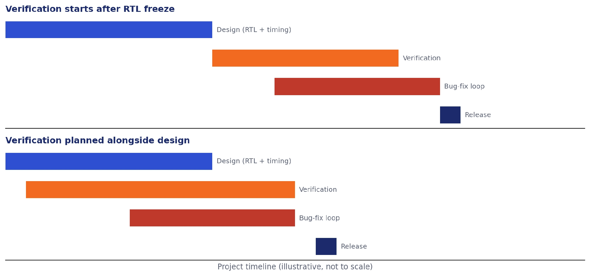
Starting verification at RTL freeze pushes the bug-fix loop to the end of the schedule. Planning it alongside design pulls the same work forward. Illustrative, not to scale.
A second common break is the same engineer doing both. When the author of a module writes its testbench, the testbench inherits the author’s blind spots. If the designer assumed the input can never exceed 1,023, the test will never send 1,024, and the overflow ships. Independence is not bureaucracy here; it is the entire point of the discipline. This is the same reasoning that separates pre-silicon and post-silicon verification into distinct stages with distinct owners.
Consider a 10G Ethernet MAC on a mid-range FPGA with a networking product. The designer writes the RTL, closes timing at 156.25 MHz, and demonstrates a clean packet passing through in simulation. It looks done. Verification then constructs a UVM environment that injects malformed frames, minimum-size 64-byte packets back to back, and a CRC error on the last byte. On the back-to-back case the design drops the second frame because an internal counter was one bit too narrow, a bug invisible in the single-packet demo and impossible to hit without targeted stimulus. That is the difference between the two disciplines in a single line: the designer proved it can work, verification proved when it does not. CRC handling rewards this kind of targeted testing, as any team that has traced CRC failures in Ethernet will recognise.
Do / Avoid
- Do: Start verification planning alongside design
- Do: Keep testbench authorship independent of RTL authors
- Do: Track functional coverage as a release gate
- Avoid: Beginning verification only after RTL freeze
- Avoid: Letting the designer sign off their own module
- Avoid: Treating timing closure as proof of correctness
A third break is measurement. Without a coverage target agreed up front, verification has no defined end. The team keeps testing until the deadline arrives rather than until a stated coverage goal is met, so the sign-off is really just the calendar running out. Agreeing that 95 percent functional coverage and 100 percent of assertions passing is the bar turns an open-ended activity into a decision anyone can audit. Write that number into the verification plan before the first testbench line exists, and both sides know what done means.
Skills and hiring: they are not interchangeable
A strong designer and a strong verification engineer are different people, and hiring one when you need the other is a common and expensive mistake. The skills overlap in language (SystemVerilog appears on both sides) but diverge sharply in mindset. Understanding the difference between FPGA design and FPGA verification at the level of who does the work is what stops you from filling a team with the wrong specialists.
Design rewards constructive thinking: how do I build this so it fits, runs fast and uses the fabric well? It leans on digital architecture, timing analysis, an understanding of block RAM, DSP slices and clocking resources, and fluency in the vendor toolchain. A designer who can read a timing report and know which of forty failing paths actually matters is worth a great deal.
Verification rewards adversarial thinking: how do I break this, and how do I prove I could not break it? It leans on methodology, UVM and constrained-random stimulus, on assertion writing, on coverage analysis, and increasingly on scripting in Python to generate tests and parse results. A verification engineer’s instinct is to distrust the happy path.
- Design skills: RTL coding, timing constraints, synthesis and place-and-route, resource optimisation, clock domain planning
- Verification skills: UVM testbench architecture, SystemVerilog assertions, functional coverage, constrained-random stimulus, protocol checking
- Shared: SystemVerilog, protocol knowledge, version control and a CI flow, reading a specification precisely
The shared column is smaller than most job descriptions imply. When you scope an FPGA team, decide the design-to-verification ratio with intention. On a control-plane heavy part with several interacting protocols, verification headcount often exceeds design headcount, sometimes running two verification engineers to one designer. On a small glue-logic FPGA the ratio can invert. Getting this wrong, staffing three designers and one verifier with an intricate part, is the single most reliable way to arrive at RTL freeze with a design nobody can prove works.
Running both disciplines through a shared CI/CD pipeline is what keeps them honest over a long programme, so that every RTL change re-runs the regression and coverage report automatically rather than waiting with a manual pass before tape-out or board bring-up. A designer who breaks a coverage point with a supposedly harmless refactor finds out overnight, not in the lab.
Design and verification answer two different questions, and a product needs both answered. Design answers can this be built and will it run. Verification answers does it do the right thing, always. Skipping or shortchanging either one does not save time; it moves the cost to the lab, where every bug is slower and dearer to find. If you are scoping an FPGA programme and are unsure whether you are short on design capacity or verification rigour, the Pqangelstech hardware engineering team can help you split the work correctly and staff it. Book a discovery call to talk through your part and your timeline.
Frequently Asked Questions
Can one engineer do both FPGA design and FPGA verification?
On small projects, yes, and it works fine. On a shipping product it is risky because the person who wrote a bug carries the same blind spots into the testbench, so the same wrong assumption goes untested. Independent verification exists precisely to catch what the designer could not imagine going wrong, which is why serious teams separate the two roles.
Is FPGA verification the same as timing closure?
No. Timing closure is a design result that proves the logic runs fast enough to meet its clock period. Verification proves the logic computes the correct answer under all expected conditions. A design can close timing perfectly and still produce wrong results on a corner case. They are independent claims, and passing one tells you nothing about the other.
Why does FPGA verification take longer than design?
Writing RTL for a feature is bounded work; proving it handles every reset, overflow, boundary and interacting condition scales with combinations, not lines of code. A state machine takes an afternoon to write and weeks to verify thoroughly. On large parts verification often consumes more calendar time and headcount than design for exactly this reason.
Do I need UVM for FPGA verification?
Not always. Small designs can be verified with directed SystemVerilog testbenches or even Python-based checks. UVM earns its cost on large parts with reusable components, constrained-random stimulus and multiple interacting protocols. For a simple glue-logic FPGA, a full UVM environment is overkill and slows you down more than it helps.
What tools do FPGA designers use versus verification engineers?
Designers work mainly in vendor implementation tools: Vivado for AMD/Xilinx parts and Quartus Prime for Intel/Altera, running synthesis and place-and-route. Verification engineers work mainly in simulators such as QuestaSim, VCS or Xcelium, plus coverage databases and scripting in Python. Both run simulation, but their centre of gravity and daily tooling differ.
Does functional coverage guarantee my FPGA design is bug free?
No. Coverage tells you which parts of the specification your tests actually exercised, not that the design is correct everywhere. You can hit 100 percent coverage and still miss a scenario the coverage model never described. It reduces risk and defines a measurable stopping point, but it is evidence of testing thoroughness, not a proof of correctness.
When should verification start in an FPGA project?
Verification planning should start alongside design, not after RTL freeze. Waiting until design finishes means the specification has drifted from the code and every bug found triggers a debate about whether it is real. Early verification planning defines coverage goals and testbench architecture while the design is still flexible enough to change cheaply.
How do I decide the design to verification headcount ratio?
Base it on the scope and scale of the system, not habit. A control-plane heavy FPGA with several interacting protocols may need two verification engineers per designer. A small glue-logic part can invert that. The reliable mistake is over-staffing design and under-staffing verification, which lands you at RTL freeze with a design nobody can prove works.
Does an ASIC verification engineer transfer easily to FPGA verification?
Mostly yes. The core skills, UVM, SystemVerilog assertions, constrained-random stimulus and coverage, transfer directly. The main adjustment is scope and turnaround: FPGA teams often run smaller testbenches and can drop into hardware faster, so some corners are checked on a board rather than exhaustively in simulation. The methodology is the same; the risk tolerance differs.
Why does my design pass simulation but fail on the actual FPGA board?
Usually because simulation tests function while the board exposes physical effects simulation ignored: clock domain crossing metastability, unconstrained false paths, reset timing, or I/O constraints that were wrong. These are design and timing issues, not functional bugs your testbench would catch. Check your constraints, cross-clock synchronisers and timing reports before assuming the RTL logic is at fault.
What is the difference between FPGA verification and FPGA validation?
Verification checks that the RTL matches its specification, mostly in simulation using testbenches, assertions and coverage. Validation checks that the design behaves correctly on real hardware, at real speed, with real software and interfaces connected. Verification finds most logic bugs early and cheaply; validation finds the system-level and interoperability problems that simulation cannot reach.
